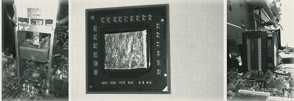
Almost 20yrs ago, my first job out of college was to get heat out of AMD's chips. We were part of a small but mighty team called “power and performance management” and our core metric was TDP – Thermal Design Power. I spent ~6yrs there working on the CPUs, APUs and GPUs you now read about in earnings calls. A lot of unglamorous afternoons clamping thermal test heads onto packages, scraping silver-colored, gluey, interface material off silicon dies, bolting heat-pipe towers onto validation boards, and treating every watt above TDP like a personal insult.
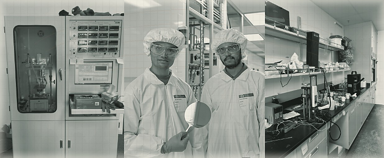
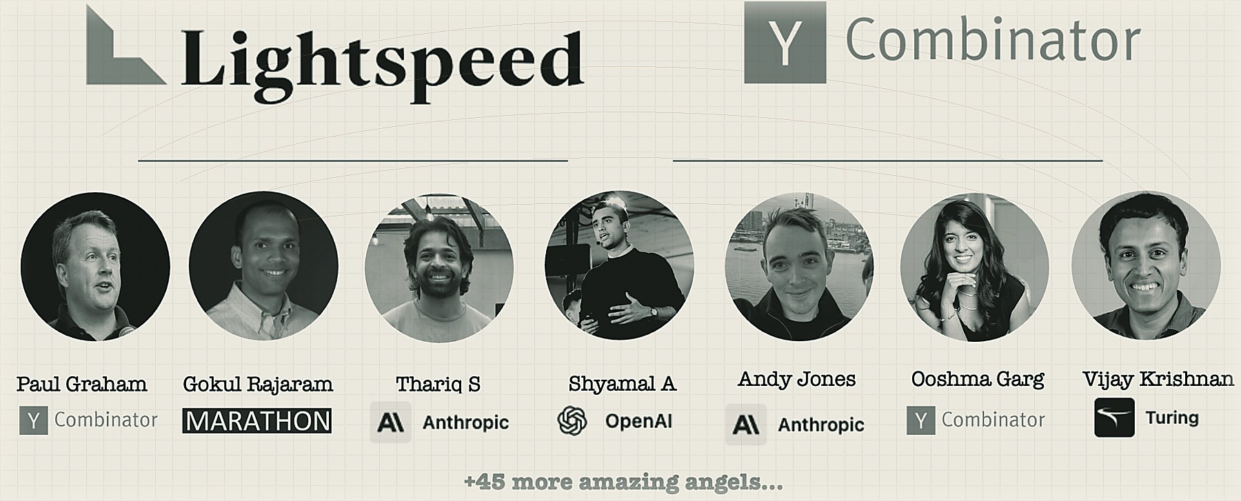
Somewhere between then and now the semiconductor industry ended up scaling 100x in almost all metrics, not just in market-cap but also the one metric that used to give us all nightmares: heat. So I consider this a bit of a personal homecoming that today we are partnering with Discovered Materials to lead their $9M seed round, joined by Y Combinator and angels such as Paul Graham, Gokul Rajaram, and leaders from the AI labs such as OpenAI, Anthropic that are deeply interested in having this problem solved. We met the founders, Advaith Sridhar and Akash Ramdas, earlier this year. This is a unique team that has spent time in Stanford's materials labs as much as in building verifiers & harnesses at frontier AI startups. Ten minutes into our first meeting we were arguing about junction temperatures and ASTM test rigs and I knew two things: this problem had finally found its team, and I was going to enjoy this diligence more than any in recent memory.
Our thesis can be easily summarized in just a few points and I’ll lay it out up-front and then, try to make Akash & Advaith proud by, as they would, empirically building a case for this investment. 1) Heat is becoming the binding constraint on AI (2) You cannot just plumb your way out of it: air-cooling, liquid-cooling, direct-to-chip cooling are all band-aids that don’t solve the core issue (3) An AI-native materials company that dissipates heat better atomically is the right, and possibly only, answer (4) The materials company will need to be closed-loop across materials discovery, a verifier that filters out unviable materials and an autonomous physical lab that rapidly synthesizes, tests, and invalidates/validates properties predicted in discovery phase.
Let’s break down every part of this thesis and build it back up. This will need a bit of a detour of physics, and asking a lot of whys.
01 - Why is Heat the binding constraint on AI?
In 2024, the bottleneck on AI was chip supply. Fast forward to 2026, most are talking about energy as the main bottleneck. There are legends of Elon Musk pushing unpermitted generators next to his datacenters to support demand scale-up on Grok. Space-based data centers are getting attention because of “free” solar power and reduced cooling needs. The real issue isn’t that more heat is getting generated; it’s that it’s getting generated over the same surface area so it’s harder to extract & dissipate it.
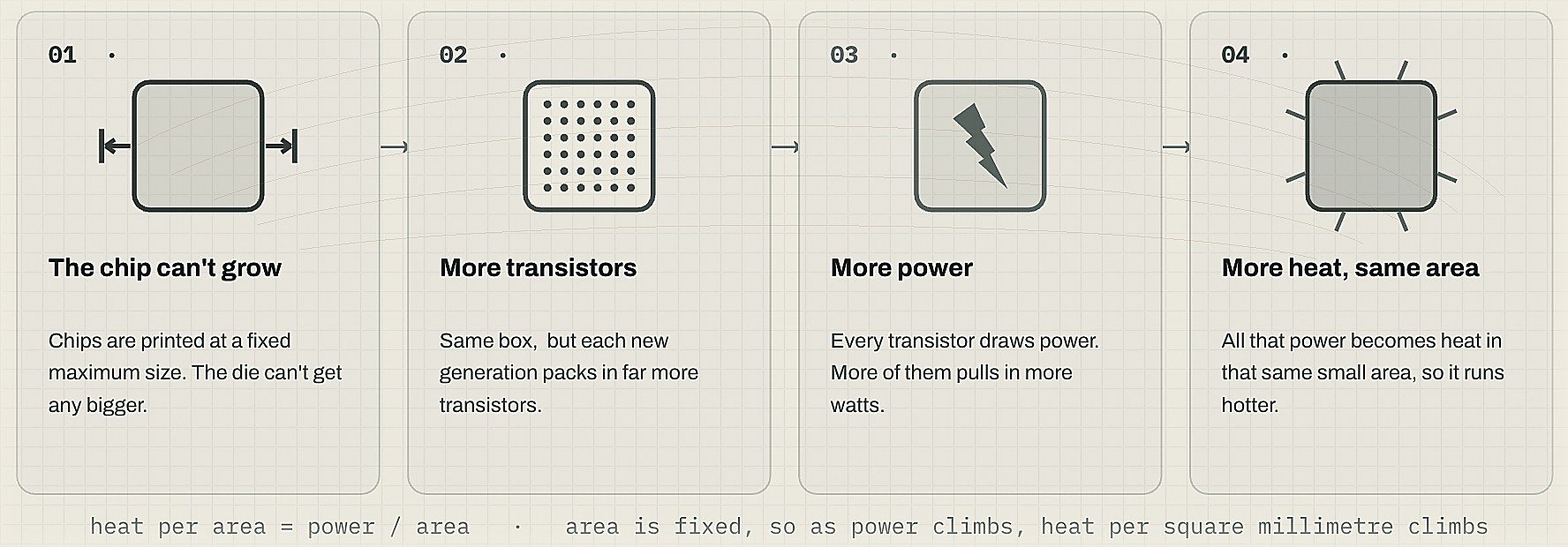
Why does the heat keep concentrating? (1) The die size cannot grow (2) Each generation therefore packs far more transistors into that same reticle-sized die to extract more TFLOPs (3) Every transistor draws power. (4) All of that power becomes heat in the same small area. Heat per area = power ÷ area and it’s elementary school math from here on: the numerator keeps growing, the denominator (per-die) stays roughly the same (the package is another story, we’ll get there in a second).
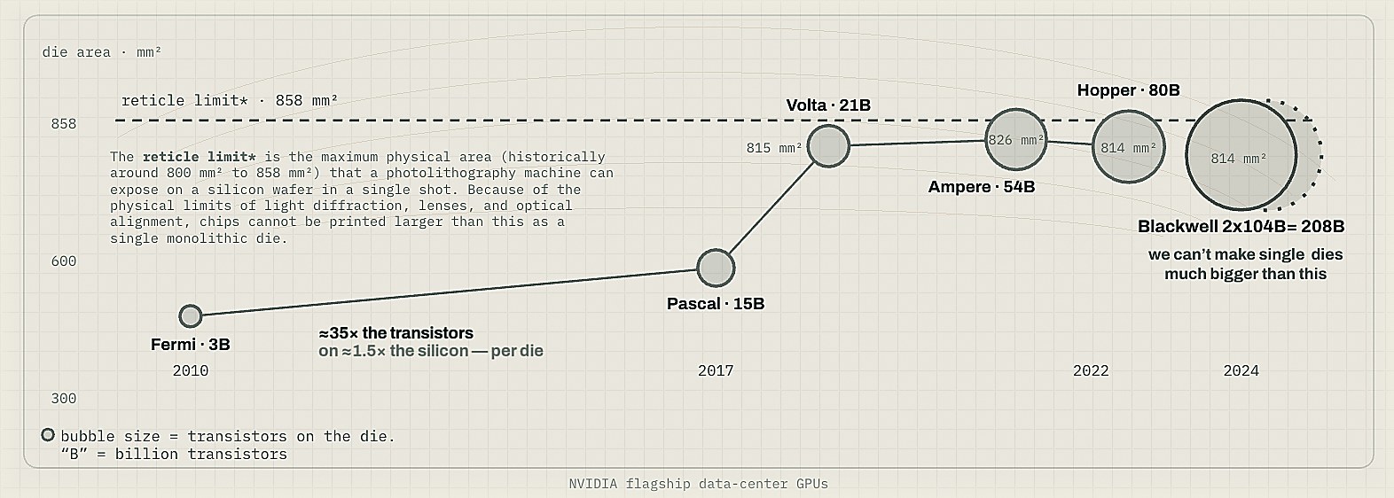
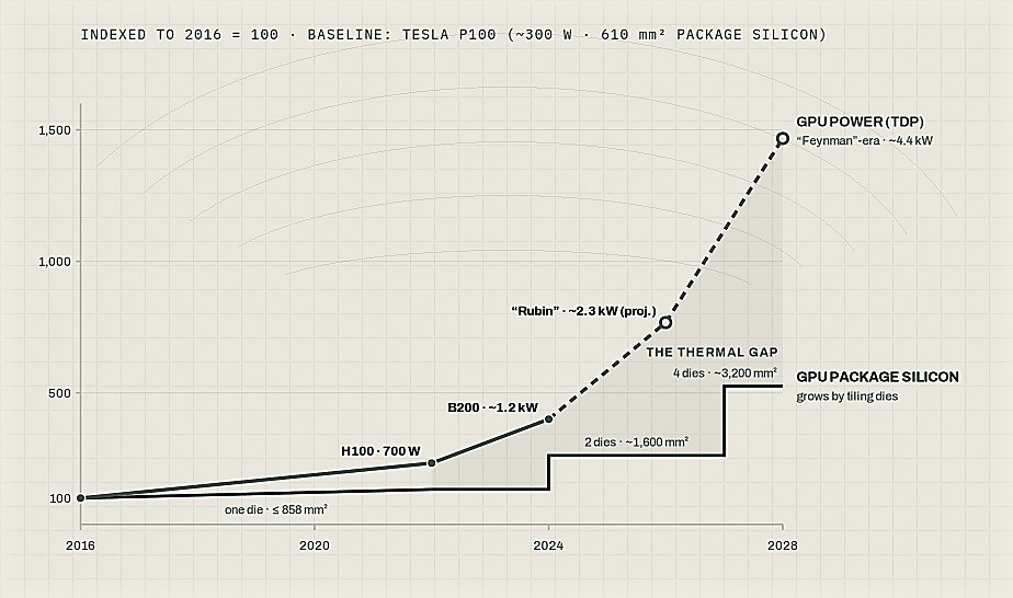
NVIDIA flagship data-center GPUs; die areas for Volta/Ampere/Hopper cluster at 814–826 mm², against a single-shot reticle limit of ≈858 mm². *Blackwell's 208B transistors span two reticle-size dies fused in one package — the clearest possible admission that the box is full.
If you are really keen to go deeper in the why-rabbithole, you may want to know why can’t the chips grow any larger – surely, that’d solve much of this issue, right? Let me introduce you to the reticle limit. The reticle limit is the maximum physical area (historically around 800 mm² to 858 mm²) that a photolithography machine can expose on a silicon wafer in a single shot. Because of the physical limits of light diffraction, lenses, and optical alignment, chips cannot be printed larger than this as a single monolithic die. As you can see below, we have been sitting at the reticle limit since early 2020s. Nvidia’s last 3 generations have gone from 54B transistors squeezed into a 826mm2 area to now 104B transistors on a 814mm2 area. And when that wasn’t enough, Blackwell fused two reticle-size dies into one package to reach 208B (~1600mm2), with Rubin Ultra set to stitch four dies together (~3200mm2). The die is pinned at the reticle but the package now grows by tiling dies. Doesn’t that solve the heat problem, you may ask? No – power is growing faster than the tiled silicon. Hopper ran 700W on one die; Blackwell ran ~1.2kW on two; Rubin- and Feynman-era parts are projected to be near 2.3kW and 4.4kW. Every added die is stitched to its neighbors through bonded interfaces where heat gets stuck.
02 Why can’t we just plumb our way out of this heat?
So far we’ve established why more heat is getting generated and why it’s getting concentrated on the same surface area making it harder to dissipate. Let’s ask the next why - why can’t we just plumb our way out of this heat? Let’s first establish just how the power needed to cool scales with generated heat.
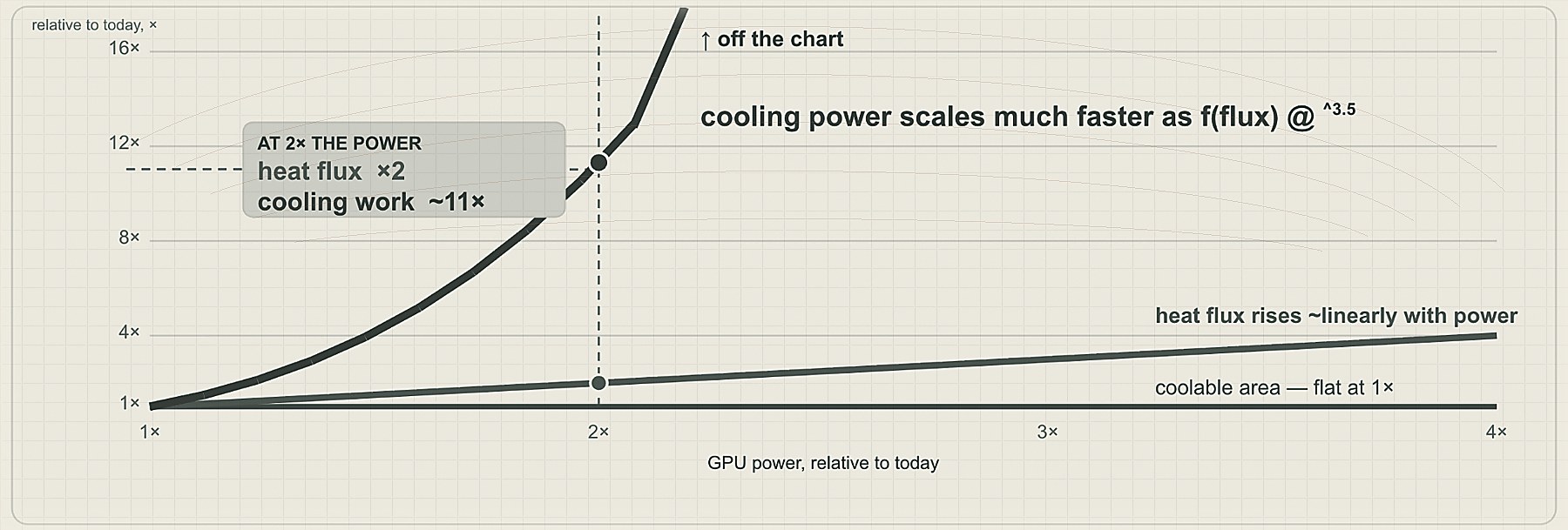
At AMD, I lived inside the above chart. Every watt we couldn't conduct away, we paid for several times over in fans, fins, pumps, and plumbing. To hold the chip's temperature fixed, the work required to remove additional generated heat doesn't rise linearly with the heat. It rises with roughly the 3.5th power of heat flux. Double the flux and you need about 11x the cooling work. Now when you put that chart above with the one below, you’d notice just how much more power is getting utilized by chips planned for the next few years. There is an entire order of magnitude difference between power needed by H100 racks vs what is planned for Rubin and Feynman. I don’t need to tell you that when you apply the 3.5^ exponent on an already 10x scale, the numbers get unmanageable very, very quickly.
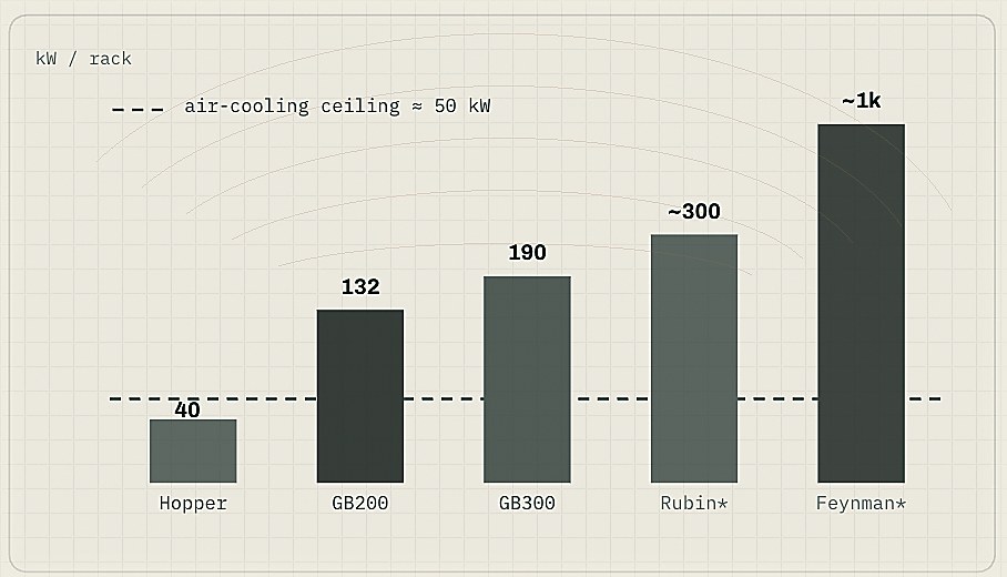
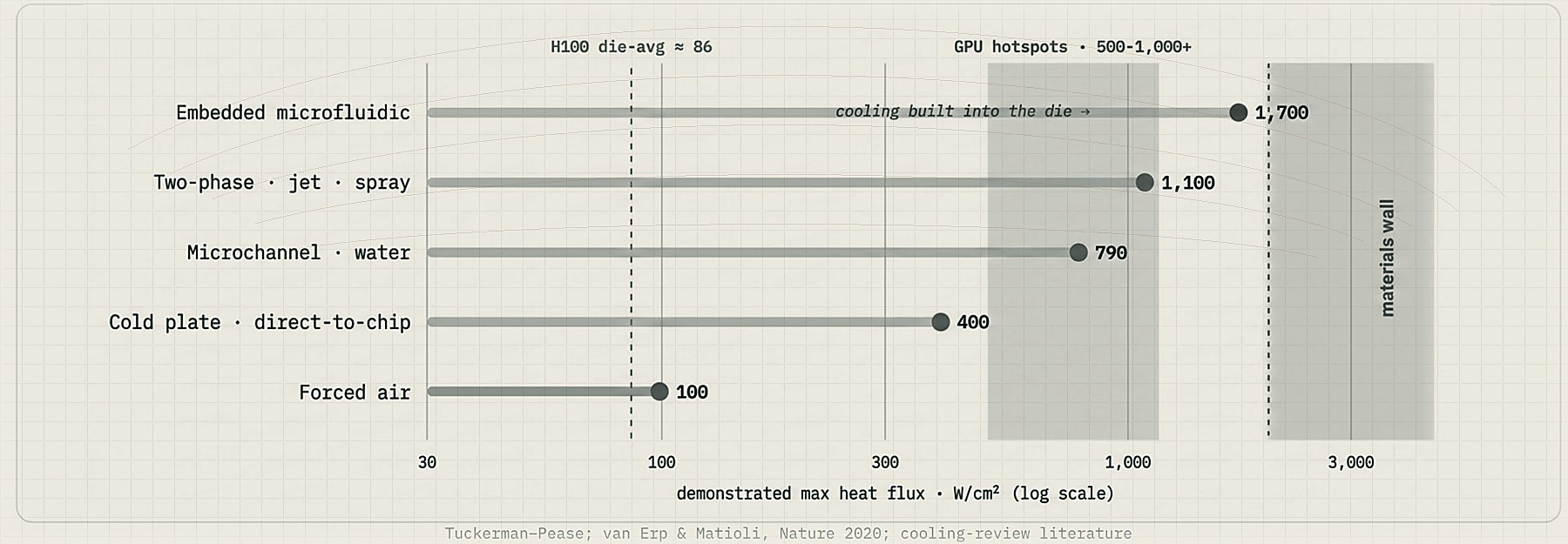
We know that air is not a good carrier of heat. On a per-rack basis, we crossed the capabilities of air-cooling (~50kW) a few generations ago. Water carries heat roughly 3,500× better than air, which is why everything above the H100 has gone to direct-to-chip liquid cooling. It helps but plumbing only solves the last leg of the journey which is getting heat out of a cold plate and into a fluid. It does nothing about the first and the hardest leg: getting heat out of the silicon and across every interface in its way. Every cooling technique ever demonstrated has a hard ceiling on the heat flux it can absorb and past roughly 2 kW/cm², pushing fluid faster does not help any more. At that point the limit is no longer the pump but rather the stack of materials standing between the transistor and the coolant.
03 Why are new materials the only answer to conduct this heat away?
Heat doesn't get stuck in the chip. It gets stuck in the gaps between things. Silicon itself conducts heat perfectly well but the problem lies in every boundary the heat must cross on the way out: die-to-lid, lid-to-heatsink, die-to-die in a stack, etc. And it gets dramatically worse the moment you stack chips e.g. 3D integration including memory on logic or die on die. This reduces the area of the GPU and is being done to reduce communication time between memory and compute units. This is the only way to get more performance while working around the current reticle limits till a new way to etch wafers are invented. But as you try to bring things closer together, no matter how close you get them, when seen under a microscope, two "flat" solid surfaces actually touch across only about 10% of their area. The rest is trapped air, and thermally speaking, air is a wall. The core tension here is communication bandwidth vs heat - bringing things closer decreases communication time, but makes the heat problem worse. The chip industry's roadmap is quite literally burying its heat problem inside the package where no cold plate can ever reach it. Only a better material can.
04 Why we need Discovered Materials
Materials discovery has always been about search. Edison famously burned through some 6,000 candidate filaments over two decades before the lightbulb had a filament worth shipping. A century and a half later, the process at the incumbents such as Dow, Henkel, 3M, Shin-Etsu and others is still recognizably that: brilliant chemists, hand-tuned formulations, quarters-to-years per cycle. Search is the bottleneck and search is the one thing modern AI has become shockingly good at.
Discovered Material’s engine runs the loop 24/7: an agent proposes ~2000+ candidate crystal structures a day; a separate, proprietary verifier model scores each for stability, heat conduction, dielectric constant, interfacial resistance, synthesizability etc in about ten minutes; physics simulation (DFT) confirms a shortlist over days; and an autonomous wet lab synthesizes and measures what survives. Design → make → measure, all of it compressed from quarters into days.
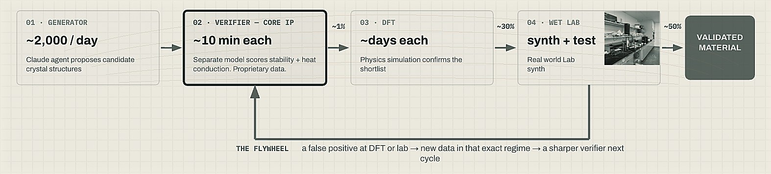
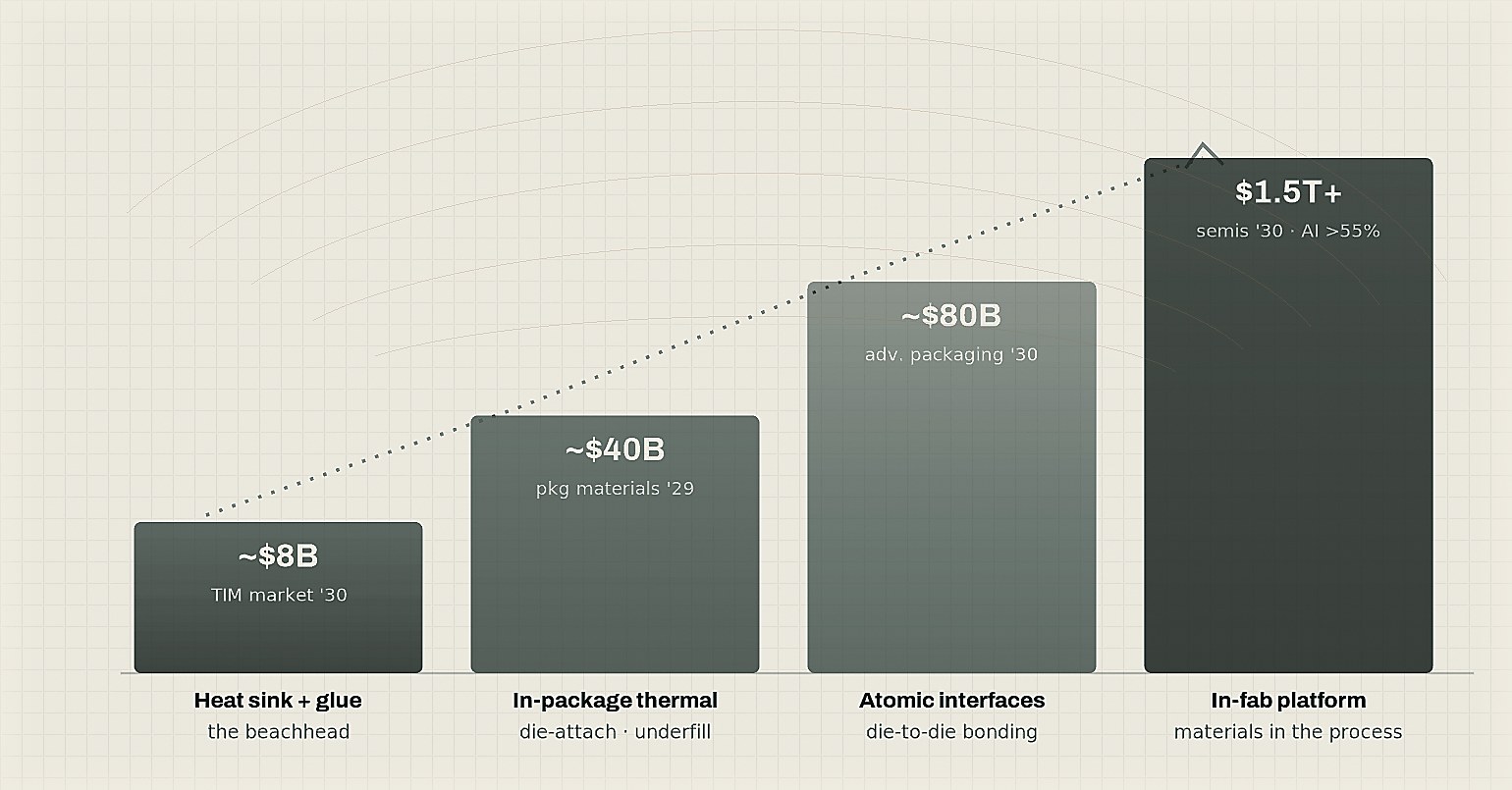
The materials verifier is the company. Proposing candidates gets cheaper with every frontier-model release and that loop is being commoditized for everyone. Knowing which of the day’s 2000+ candidates deserves a wet-lab run is not easy, and never will be. Discovered’s verifier is trained on a proprietary thermal-conductivity dataset larger than the Materials Project. Tune the sieve too wide and your lab budget explodes; too narrow and you filter out the winner. Getting that balance right is the moat. Is it working? In their YC batch, the team went from a cold start to matching Dow's commercial TIM performance in about six weeks, beating a Henkel reference along the way. That said, the TIM market is small at ~$4B today, maybe $8B by 2030, and mostly consumer and automotive at that. TIMs are maybe 10% of the heat problem. They are the beachhead and the material’s discovery engine into higher value categories such as in-package thermal-materials, to atomic-width interfaces in advanced packaging where 3D stacked silicon is headed; and ultimately into materials specified inside the fab process itself, in a semiconductor market headed well past $1.5T with AI driving >50% of that growth.
1,000,000× - the end game
Our brains do their thinking on about 20 watts which is a million-fold efficiency gap between biology and the GPU racks we are building. Adding more registers to the die adds more TFLOPs to the chip. In a way, it helps you grow a bigger, more powerful brain. The opposing force here is heat. As chips get hotter, they automatically trigger thermal throttling i.e. chips actively lowers their clock speeds and voltages to cool down and prevent permanent hardware damage. Every new TFLOP we add to the world is being gate-kept by the heat it generates. This is why the work Discovered Materials is doing is so critical. Within three years, we believe no frontier accelerator will ship without an AI-discovered material somewhere in its heat path.
The founders of Discovered Materials have done exactly this work in the past. In January 2025, Akash and his Stanford collaborators published in Science a genuinely surprising result: an ultrathin niobium-phosphide semi-metal whose electrical resistivity falls as the film gets thinner – the exact opposite of copper, whose resistivity blows up in nanoscale wires. At 1.5 nm their films reached ~34 µΩ·cm, several times better than conventional metals at that scale, deposited at 400 °C which is cool enough for real chip manufacturing. It was Stanford Engineering's most-read story of 2025. Note what that work attacks: the resistive generation of heat inside interconnects. DiscoveredMaterials attacks heat's dissipation and generation. Twenty years after I left this problem back at AMD the entire AI build-out has circled back to the first problem I ever owned professionally. Backing the team that has published at the atomic scale on both sides of the heat equation before raising a seed round is so rare and is about as close to a homecoming as this job allows.
We're delighted to partner with Y Combinator and with angels from the labs and firms building the frontier. Welcome to the Lightspeed family, Advaith and Akash.
No comments yet.